|
1.
What is the general lead-time of the products?
Generally, if the crystal needed has raw material in
stock, the lead-time may be sooner than expect. If the
parts or raw material are not available and need to
be made from scratch. The general lead-time is as follow:
| Crystal |
3
~ 4 weeks |
| Clock
Oscillator |
6
~ 8 weeks |
| TCXO |
8
~ 12 weeks |
| VCXO |
6
~ 10 weeks |
| VCTCXO |
8
~ 12 weeks |
(*Lead-time
may vary from time to time. Please double confirm.)
2.
Since the lead-time is set, what about sampling?
For prototyping, we normally would search our inventory
for a similar part that matches the custom part's requirement.
The manufacturing of the custom part will begin the
same time if requested.
3.
What basic information to provide when ordering a crystal?
Generally we request the customer to provide the nominal
frequency, type of cutting angle (AT/BT), holder or
package type, resistance (ESR), frequency tolerance,
frequency stability, load capacitance, operating temperature
range, drive power, aging, etc¡K Customer can
also specify other specific spec or requirement, if
any, when placing orders.
4.
What is the main difference between frequency tolerance
and frequency stability?
The frequency stability is the maximum allowable frequency
deviation, over a specified operating temperature range,
from the "reference" frequency. The
"reference" frequency is usually referred
to the resonant frequency of a crystal at room temperature
(+25¢XC)
Sometimes
the "reference" frequency may be referred
to the nominal (spec) frequency, if it is so specified
by customers.
The
frequency stability is usually stated in parts per million
(ppm).
The
frequency tolerance of a crystal is defined as the maximum
allowable frequency deviation, in ppm, from the nominal
(spec) frequency at a specified temperature, usually
+25¢XC (¡Ó2¢XC)
5.
What happens to the performance of a crystal when it's
not operating within the temperature range stated in
the specification?
The crystal performance will be affected. We highly
do not recommend such to take place. It can cause the
frequency of the crystal to drift. Worse scenario is
it may cause malfunction of customer circuit.
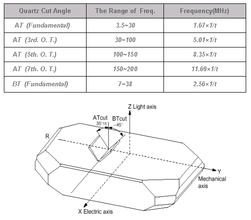
6.
What is AT or BT Cuts?
Crystal carries, mainly, its "frequency stability"
characteristics as a result of how the quartz bars are
cut, in a certain pre-oriented angle, into crystal wafers.
Today the most popular and widely used one is the AT-Cut.
The
AT-cut has a cutting angle of around 35¢X15' to
the Z-axis in the negative Y-axis direction, as compared
to a -45¢X to the Z-axis in the positive Y-axis
direction for the BT-cut. For ease of understanding,
a graph of the two cuts are shown below.
Generally
the BT cut blanks are thicker than the AT Cut one at
the same frequency, so higher frequency can be achieved
using BT cut.
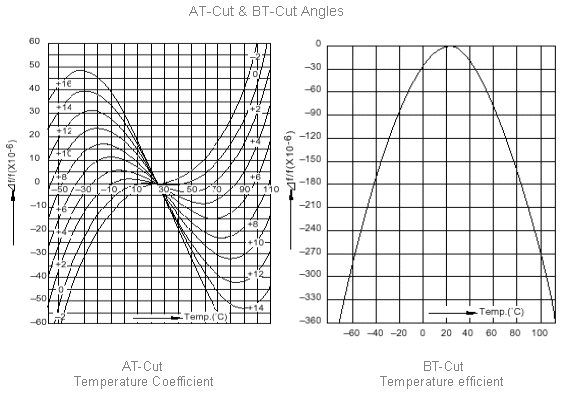
One
major difference between AT-cut and BT-cut is the frequency
stability characteristics. Please also refer to the
temperature coefficient curves of the two cuts below.
7. Does SQC make it's own crystal or do you source
and mark the parts with your name on it?
SQC is an end-to-end frequency quartz manufacturer.
By saying end-to- end, we mean not only do we make our
own crystals, we also grow our own high Q crystal bars.
8.
What is the aging of the crystal?
Aging is the change in frequency of a crystal over time.
Aging can be in the positive or negative direction.
Aging effect contributes to the overall frequency drift
of the oscillator that the crystal is used in.
Aging
will be mainly affected by two important factors, namely,
contamination and stress. Experiment proves that contamination
on crystal wafer usually causes a negative frequency
shift, whereas excessive stress often results in positive
frequency drift.
When
crystal wafer is mounted on a holder (base), it could
very possibly be pushed, pulled, or twisted by the mounting
structure. This causes stress on the crystal wafer.
Such stress will be released or relaxed with time and
thus results in positive frequency shift. When assembling
the crystal unit, proper mounting method of wafer and
using the proper holder (base) will help eliminate or
reduce the unwanted stress. For a finished crystal,
thermal cycling can be used to expedite the process
of exercising & relaxing the mounting stress.
Contamination
on wafer could happen in various stages of crystal production.
Contamination that attaches itself to the surface of
wafer causes negative frequency shift because of mass
loading effect. Contamination should be minimized by
improving cleanliness of manufacturing process as well
as cleanliness of wafer in every production step.
Crystals
can be "pre-aged", to a certain degree, to
minimize the effects of aging. Because aging characteristics
tend to follow a logarithmic curve, most of the aging
of a crystal will occur in the first year of its life.
The rate of change of crystal frequency is relatively
more or faster during the first year than the second
year and beyond.
9.
What is pull-ability?
The pull-ability of a crystal is a measure of
frequency change as a function of load capacitance.
Circuit
designer can accomplish an operating frequency range
by changing or varying the load capacitance of the crystal.
The operating frequency range is determined by the pull-ability
of the crystal at a given (varying) range of the load
capacitance.
10.
What are spurious frequencies?
It is possible for a crystal to vibrate at frequencies
that are not related to its fundamental nor overtone
frequencies. Such unwanted frequencies are referred
to as spurious.
Effects
of spurious frequencies can be suppressed in the crystal
design & manufacturing stage by changing crystal
wafer size, electrode pattern design, and adjustment
of metalization on crystal wafer.
11.
What will be the effect of spurious frequencies?
When signal level of spurious mode gets as strong as
the main mode, the oscillator may run on the spurious
mode instead of the main mode. Such a phenomenon is
called mode hopping.
Spurious
mode is usually defined as either a resistance ratio
or dB suppression to the main mode. A resistance ratio
of 1.5 or 2.0 to that of the main mode is needed to
avoid mode hopping for most oscillators. This would
be approximately equivalent to a -3dB to -6dB signal
suppression over the main mode.
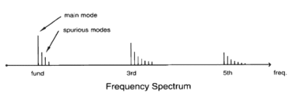
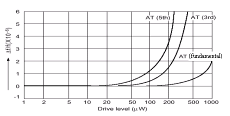
12.
What happens if I operate a crystal over its maximum
drive level spec?
An over-drive crystal may cause its frequency and resistance
to change, in many cases, to a higher value. This would
mean changes in crystal electrical characteristics.
Sometimes activity dips could thus happen. It could
also result in a broken crystal wafer due to too much
power over-drive for too long an interval of time.
A
common phenomenon in frequency shift over high drive
power is depicted below.
13.
What is an activity dip and do I need to worry about
them?
Activity dips are symptoms of discontinuity in frequency
or resistance of a crystal over its operating temperature
range. Sometimes it is also referred to as "non-linearity".
Depending
on the real circuit implementation, different circuit
designs may tolerate different levels of crystal activity
dips.
Many
possible factors would contribute to activity dips,
including, but not limited to, dirt on crystal blank,
cracks on the edge of crystal blank, inappropriate design
of blank dimension, poor stickness in metalization layers,
high humidity inside the crystal enclosure, etc. Activity
dips can be effectively suppressed by improvement in
the above-mentioned areas during crystal production.
14.
Why don't HC-49S crystals pull as much as HC-49U crystals?
Pull-ability of a crystal usually has to do with the
electrode size which forms on the crystal blank. A bigger
size crystal blank of course can accommodate a larger
electrode. HC-49S has a smaller dimension in blank than
HC-49U.
Larger
electrode would typically provide a wider frequency
pulling range when crystal is placed in series with
a given load capacitance in the oscillation circuit.
15.
What is trim sensitivity (T.S.)?
Trim sensitivity is the incremental frequency change
of a crystal for an increment change in load capacitance.
It is often expressed in ppm/pF. A typical mathematical
approximation for trim sensitivity shows T.S. changes
as CL varies:
T.S.=
C1 / [ 2 (Co+CL) ]
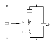
16.
What are the motional and shunt capacitances of a crystal
unit?
Motional capacitance (C1):
It is the capacitance residing in the motional (series)
arm
of the ideal crystal equivalent circuit model.
Shunt
capacitance (C0):
It is the static capacitance between the crystal electrodes,
together with the stray capacitance of the mounting
system.
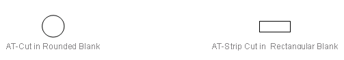
17.
What are the differences between AT-cuts and AT-strip
cuts?
Please also refer to FAQ No. 6 for explanation on AT-Cut.
AT-strip
cut is usually referred to the rectangular crystal blanks
which have the AT-Cut angle.
18.
What is the difference between a "crystal"
and a "strip resonator"?
A strip resonator is a crystal in which an AT-strip
cut blank is used and mounted.
A
strip resonator is more sophisticated in its electrical
characteristics than a crystal that utilizes a round
blank. More skills and cautions are required in the
design for a strip resonator to achieve the desired
electrical characteristics.
19.
What is load capacitance?
Crystal by its function is to be placed and work in
an oscillation circuit for generating a desired oscillation
frequency. When a crystal sits in an oscillation circuit,
it sees a "load capacitance" at the two terminal
leads of the crystal. Such a load capacitance is the
equivalent capacitive effect of the entire oscillation
circuitry that appears at or presents to the crystal.
Thus,
the nominal spec frequency of a crystal is often defined
as FL which stands for "load resonant frequency"
at a given capacitance value. This capacitance value
is to reflect the actual "load capacitance"
presented to the crystal when it is placed and work
in a real oscillation circuit.
A
crystal with zero (0) load capacitance number has its
resonate frequency designated as Fr, series resonant
frequency.
20.
What are piezoelectric characteristics of a quartz crystal
unit?
Quartz is a device that carries the piezoelectric characteristics.
The piezoelectric characteristics of a quartz crystal
is briefly explained below:
If
a piezoelectric quartz crystal has electrodes plated
on opposite faces and if a potential is applied between
these electrodes, forces will be exerted on the bound
charges within the crystal. If the crystal is properly
mounted, deformations take place within the crystal,
and an electromechanical system is formed which will
vibrate at a resonant frequency when properly excited.
21.
What are electrode, base plating, fine plating and plate
back for crystal?
Each crystal has a blank inside the enclosure. There
are two electrodes on the blank, one on each side of
the blank. The electrode is a round or rectangular area
covered by a thin layer of silver (in some designs,
it could be gold/Ag too). In crystal production, the
electrodes were formed by deposition of silver onto
the blank in high vacuum. This process is also known
as "plating".
Forming the electrode on the blank is actually a process
of plating (depositing) silver onto the blank. Plating
is done in two steps, base plating and fine plating.
Base plating is performed in a batch mode by which a
bunch of blanks are plated at the same time in one vacuum
chamber. Base plating usually brings the blanks to a
frequency range that is roughly 500 to 1,000 ppm (plate
back range) above the target frequency. Fine
plating is then done one by one and it will precisely
take each blank to within, for example, +/- 30 ppm tolerance
of the spec (target) frequency.
|